


High-performance self-driven infrared photodetector
infrared photodetector has the characteristics of strong anti-interference ability, strong target recognition ability, all-weather operation and good concealment. It is playing an increasingly important role in fields such as medicine, military, space technology and environmental engineering. Among them, the self-driven photoelectric detection chip that can operate independently without an external additional power supply has attracted extensive attention in the field of infrared detection due to its unique performance (such as energy independence, high sensitivity and stability, etc.). In contrast, traditional photoelectric detection chips, such as silicon-based or narrowbandgap semiconductor-based infrared chips, not only require additional bias voltages to drive the separation of photogenerated carriers to produce photocurrents, but also need additional cooling systems to reduce thermal noise and improve responsiveness. Therefore, it has become difficult to meet the new concepts and requirements of the next generation of infrared detection chips in the future, such as low power consumption, small size, low cost and high performance.
Recently, research teams from China and Sweden have proposed a novel p-i-n heterojunction self-driven short-wave infrared (SWIR) photoelectric detection chip based on graphene nanoribbon (GNR) films/alumina/single crystal silicon. Under the combined effect of the optical gating effect triggered by the heterogeneous interface and the built-in electric field, the chip demonstrated ultra-high response and detection performance at zero bias voltage. The photoelectric detection chip has A response rate as high as 75.3 A/W in self-driven mode, a detection rate of 7.5 × 10¹⁴ Jones, and an external quantum efficiency close to 104%, improving the detection performance of the same type of silicon-based chips by a record 7 orders of magnitude. In addition, under the conventional drive mode, the chip’s response rate, detection rate, and external quantum efficiency are all as high as 843 A/W, 10¹⁵ Jones, and 105% respectively, all of which are the highest values reported in current research. Meanwhile, this research also demonstrated the real-world application of the photoelectric detection chip in the fields of optical communication and infrared imaging, highlighting its huge application potential.
In order to systematically study the photoelectric performance of the photodetector based on graphene nanoribbons /Al₂O₃/ single crystal silicon, researchers tested its static (current-voltage curve) and dynamic characteristic responses (current-time curve). To systematically evaluate the optical response characteristics of the graphene nanoribbon /Al₂O₃/ monocrystalline silicon heterostructure photodetector under different bias voltages, researchers measured the dynamic current response of the device at 0 V, -1 V, -3 V and -5 V biases, with an optical power density of 8.15 μW/cm². The photocurrent increases with the reverse bias and shows a fast response speed at all bias voltages.
Finally, the researchers fabricated an imaging system and successfully achieved self-powered imaging of short-wave infrared. The system operates under zero bias and has no energy consumption at all. The imaging capability of the photodetector was evaluated using a black mask with the letter “T” pattern (as shown in Figure 1).
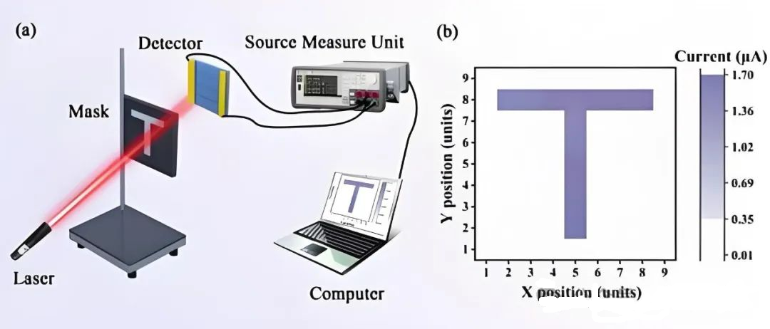
In conclusion, this research successfully fabricated self-powered photodetectors based on graphene nanoribbons and achieved a record-breaking high response rate. Meanwhile, the researchers successfully demonstrated the optical communication and imaging capabilities of this highly responsive photodetector. This research achievement not only provides a practical approach for the development of graphene nanoribbons and silicon-based optoelectronic devices, but also demonstrates their excellent performance as self-powered short-wave infrared photodetectors.
Post time: Apr-28-2025