


Single-photon photodetector have broken through the 80% efficiency bottleneck
Single-photon photodetector are widely used in the fields of quantum photonics and single-photon imaging due to their compact and low-cost advantages, but they are confronted with the following technical bottlenecks.
Current technical limitations
1.CMOS and thin-junction SPAD: Although they have high integration and low timing jitter, the absorption layer is thin (a few micrometers), and the PDE is limited in the near-infrared region, with only about 32% at 850 nm.
2. Thick-junction SPAD: It features an absorption layer tens of micrometers thick. Commercial products have a PDE of approximately 70% at 780 nm, but breaking through 80% is extremely challenging.
3. Read out circuit limitations: Thick-junction SPAD requires an overbias voltage of over 30V to ensure a high avalanche probability. Even with a quenching voltage of 68V in traditional circuits, the PDE can only be increased to 75.1%.
Solution
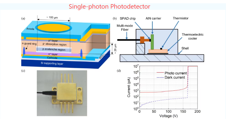
Optimize the semiconductor structure of SPAD. Back-illuminated design: Incident photons decay exponentially in silicon. The back-illuminated structure ensures that the majority of photons are absorbed in the absorption layer, and the generated electrons are injected into the avalanche region. Because the ionization rate of electrons in silicon is higher than that of holes, electron injection provides a higher probability of avalanche. Doping compensation avalanche region: By using the continuous diffusion process of boron and phosphorus, the shallow doping is compensated to concentrate the electric field in the deep region with fewer crystal defects, effectively reducing noise such as DCR.
2. High-performance readout circuit. 50V high amplitude quenching Fast state transition; Multimodal operation: By combining FPGA control QUENCHING and RESET signals, flexible switching between free operation (signal trigger), gating (external GATE drive), and hybrid modes is achieved.
3. Device preparation and packaging. The SPAD wafer process is adopted, with a butterfly package. The SPAD is bonded to the AlN carrier substrate and vertically installed on the thermoelectric cooler (TEC), and temperature control is achieved through a thermistor. Multimode optical fibers are precisely aligned with the SPAD center to achieve efficient coupling.
4. Performance calibration. Calibration was carried out using a 785 nm picosecond pulsed laser diode (100 kHz) and a time-digital converter (TDC, 10 ps resolution).
Summary
By optimizing the SPAD structure (thick junction, back-illuminated, doping compensation) and innovating the 50 V quenching circuit, this study successfully pushed the PDE of the silicon-based single-photon detector to a new height of 84.4%. Compared with commercial products, its comprehensive performance has been significantly enhanced, providing practical solutions for applications such as quantum communication, quantum computing, and high-sensitivity imaging that require ultra-high efficiency and flexible operation. This work has laid a solid foundation for the further development of silicon-based single-photon detector technology.
Post time: Oct-28-2025