


SPAD single-photon avalanche photodetector
When SPAD photodetector sensors were first introduced, they were mainly used in low-light detection scenarios. However, with the evolution of their performance and the development of scene requirements, SPAD photodetector sensors have been increasingly applied in consumer scenarios such as automotive radars, robots, and unmanned aerial vehicles. Due to its high sensitivity and low noise characteristics, the SPAD photodetector sensor has become an ideal choice for achieving high-precision depth perception and low-light imaging.
Unlike traditional CMOS image sensors (CIS) based on PN junctions, the core structure of SPAD photodetector is an avalanche diode operating in Geiger mode. From the perspective of physical mechanisms, the complexity of SPAD photodetector is significantly higher than that of PN junction devices. This is mainly reflected in the fact that under high reverse bias, it is more likely to cause problems such as the injection of unbalanced carriers, thermal electron effects, and tunneling currents assisted by defect states. These characteristics make it face severe challenges at the design, process, and circuit architecture levels.
Common performance parameters of SPAD avalanche photodetector include Pixel Size (Pixel Size), dark count noise (DCR), light detection probability (PDE), dead Time (DeadTime), and Response time (Response Time). These parameters directly affect the performance of the SPAD avalanche photodetector. For instance, the dark count rate (DCR) is a key parameter for defining detector noise, and the SPAD needs to maintain a bias higher than the breakdown to function as a single-photon detector. The probability of light detection (PDE) determines the sensitivity of SPAD avalanche photodetector and is affected by the intensity and distribution of the electric field. In addition, the DeadTime is the time required for the SPAD to return to its initial state after being triggered, which affects the maximum photon detection rate and dynamic range.
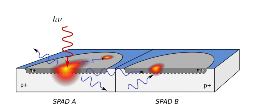
In the performance optimization of SPAD devices, the constraint relationship among core performance parameters is a major challenge: for instance, pixel miniaturization directly leads to PDE attenuation, and the concentration of edge electric fields caused by size miniaturization will also cause a sharp increase in DCR. Reducing the dead time will induce post-impulse noise and deteriorate the accuracy of time jitter. Now, the cutting-edge solution has achieved a certain degree of collaborative optimization through methods such as DTI/ protection loop (suppressing crosstalk and reducing DCR), pixel optical optimization, introduction of new materials (SiGe avalanche layer enhancing infrared response), and three-dimensional stacked active quenching circuits.
Post time: Jul-23-2025