


Choice of ideal laser source: edge emission semiconductor laser
1. Introduction
Semiconductor laser chips are divided into edge emitting laser chips (EEL) and vertical cavity surface emitting laser chips (VCSEL) according to the different manufacturing processes of resonators, and their specific structural differences are shown in Figure 1. Compared with vertical cavity surface emitting laser, edge emitting semiconductor laser technology development is more mature, with a wide wavelength range, high electro-optical conversion efficiency, large power and other advantages, very suitable for laser processing, optical communication and other fields. At present, edge-emitting semiconductor lasers are an important part of the optoelectronics industry, and their applications have covered industry, telecommunications, science, consumer, military and aerospace. With the development and progress of technology, the power, reliability and energy conversion efficiency of edge-emitting semiconductor lasers have been greatly improved, and their application prospects are more and more extensive.
Next, I will lead you to further appreciate the unique charm of side-emitting semiconductor lasers.
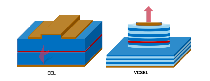
Figure 1 (left) side emitting semiconductor laser and (right) vertical cavity surface emitting laser structure diagram
2. Working principle of edge emission semiconductor laser
The structure of edge-emitting semiconductor laser can be divided into the following three parts: semiconductor active region, pump source and optical resonator. Different from the resonators of vertical cavity surface-emitting lasers (which are composed of top and bottom Bragg mirrors), the resonators in edge-emitting semiconductor laser devices are mainly composed of optical films on both sides. The typical EEL device structure and resonator structure are shown in Figure 2. The photon in the edge-emission semiconductor laser device is amplified by mode selection in the resonator, and the laser is formed in the direction parallel to the substrate surface. Edge-emitting semiconductor laser devices have a wide range of operating wavelengths and are suitable for many practical applications, so they become one of the ideal laser sources.
The performance evaluation indexes of edge-emitting semiconductor lasers are also consistent with other semiconductor lasers, including: (1) laser lasing wavelength; (2) Threshold current Ith, that is, the current at which the laser diode begins to generate laser oscillation; (3) Working current Iop, that is, the driving current when the laser diode reaches the rated output power, this parameter is applied to the design and modulation of the laser drive circuit; (4) Slope efficiency; (5) Vertical divergence Angle θ⊥; (6) Horizontal divergence Angle θ∥; (7) Monitor the current Im, that is, the current size of the semiconductor laser chip at the rated output power.
3. Research progress of GaAs and GaN based edge emitting semiconductor lasers
The semiconductor laser based on GaAs semiconductor material is one of the most mature semiconductor laser technologies. At present, GAAS-based near-infrared band (760-1060 nm) edge-emitting semiconductor lasers have been widely used commercially. As the third generation semiconductor material after Si and GaAs, GaN has been widely concerned in scientific research and industry because of its excellent physical and chemical properties. With the development of GAN-based optoelectronic devices and the efforts of researchers, GAN-based light-emitting diodes and edge-emitting lasers have been industrialized.
Post time: Jan-16-2024