


High linearity electro-optic modulator and microwave photon application
With the increasing requirements of communication systems, in order to further improve the transmission efficiency of signals, people will fuse photons and electrons to achieve complementary advantages, and microwave photonics will be born. The electro-optical modulator is needed for the conversion of electricity to light in microwave photonic systems, and this key step usually determines the performance of the whole system. Since the conversion of radio frequency signal to optical domain is an analog signal process, and ordinary electro-optical modulators have inherent nonlinearity, there is serious signal distortion in the conversion process. In order to achieve approximate linear modulation, the operating point of the modulator is usually fixed at the orthogonal bias point, but it still cannot meet the requirements of microwave photon link for the linearity of the modulator. Electro-optic modulators with high linearity are urgently needed.
The high-speed refractive index modulation of silicon materials is usually achieved by the free carrier plasma dispersion (FCD) effect. Both the FCD effect and PN junction modulation are nonlinear, which makes the silicon modulator less linear than the lithium niobate modulator. Lithium niobate materials exhibit excellent electro-optical modulation properties due to their Pucker effect. At the same time, lithium niobate material has the advantages of large bandwidth, good modulation characteristics, low loss, easy integration and compatibility with semiconductor process, the use of thin film lithium niobate to make high-performance electro-optical modulator, compared with silicon almost no “short plate”, but also to achieve high linearity. Thin film lithium niobate (LNOI) electro-optic modulator on insulator has become a promising development direction. With the development of thin film lithium niobate material preparation technology and waveguide etching technology, the high conversion efficiency and higher integration of thin film lithium niobate electro-optic modulator has become the field of international academia and industry.
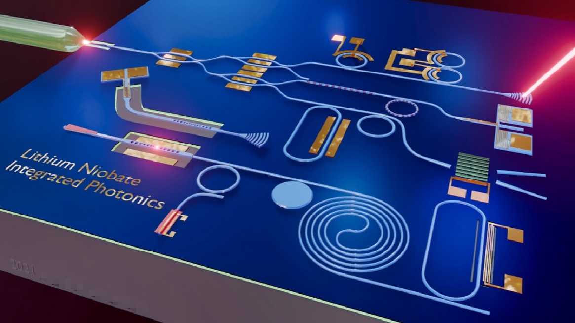
Characteristics of thin film lithium niobate
In the United States DAP AR planning has made the following evaluation of lithium niobate materials: if the center of the electronic revolution is named after the silicon material that makes it possible, then the birthplace of the photonics revolution is likely to be named after lithium niobate. This is because lithium niobate integrates electro-optical effect, acousto-optical effect, piezoelectric effect, thermoelectric effect and photorefractive effect in one, just like silicon materials in the field of optics.
In terms of optical transmission characteristics, InP material has the largest on-chip transmission loss due to the absorption of light in the commonly used 1550nm band. SiO2 and silicon nitride have the best transmission characteristics, and the loss can reach the level of ~ 0.01dB/cm; At present, the waveguide loss of thin-film lithium niobate waveguide can reach the level of 0.03dB/cm, and the loss of thin-film lithium niobate waveguide has the potential to be further reduced with the continuous improvement of the technological level in the future. Therefore, the thin film lithium niobate material will show good performance for passive light structures such as photosynthetic path, shunt and microring.
In terms of light generation, only InP has the ability to emit light directly; Therefore, for the application of microwave photons, it is necessary to introduce the InP based light source on the LNOI based photonic integrated chip by the way of backloading welding or epitaxial growth. In terms of light modulation, it has been emphasized above that thin film lithium niobate material is easier to achieve larger modulation bandwidth, lower half-wave voltage and lower transmission loss than InP and Si. Moreover, the high linearity of electro-optical modulation of thin film lithium niobate materials is essential for all microwave photon applications.
In terms of optical routing, the high speed electro-optical response of thin film lithium niobate material makes the LNOI based optical switch capable of high-speed optical routing switching, and the power consumption of such high-speed switching is also very low. For the typical application of integrated microwave photon technology, the optically controlled beamforming chip has the ability of high-speed switching to meet the needs of fast beam scanning, and the characteristics of ultra-low power consumption are well adapted to the strict requirements of large-scale phased array system. Although the InP based optical switch can also realize high-speed optical path switching, it will introduce large noise, especially when the multilevel optical switch is cascaded, the noise coefficient will be seriously deteriorated. Silicon, SiO2 and silicon nitride materials can only switch optical paths through the thermo-optical effect or carrier dispersion effect, which has the disadvantages of high power consumption and slow switching speed. When the array size of the phased array is large, it cannot meet the requirements of power consumption.
In terms of optical amplification, the semiconductor optical amplifier (SOA) based on InP has been mature for commercial use, but it has the disadvantages of high noise coefficient and low saturation output power, which is not conducive to the application of microwave photons. The parametric amplification process of thin-film lithium niobate waveguide based on periodic activation and inversion can achieve low noise and high power on-chip optical amplification, which can well meet the requirements of integrated microwave photon technology for on-chip optical amplification.
In terms of light detection, the thin film lithium niobate has good transmission characteristics to light in 1550 nm band. The function of photoelectric conversion cannot be realized, so for microwave photon applications, in order to meet the needs of photoelectric conversion on the chip. InGaAs or Ge-Si detection units need to be introduced on LNOI based photonic integrated chips by backloading welding or epitaxial growth. In terms of coupling with optical fiber, because the optical fiber itself is SiO2 material, the mode field of SiO2 waveguide has the highest matching degree with the mode field of optical fiber, and the coupling is the most convenient. The mode field diameter of the strongly restricted waveguide of thin film lithium niobate is about 1μm, which is quite different from the mode field of optical fiber, so proper mode spot transformation must be carried out to match the mode field of optical fiber.
In terms of integration, whether various materials have a high integration potential depends mainly on the bending radius of the waveguide (affected by the limitation of the waveguide mode field). The strongly restricted waveguide allows a smaller bending radius, which is more conducive to the realization of high integration. Therefore, thin-film lithium niobate waveguides have the potential to achieve high integration. Therefore, the appearance of thin film lithium niobate makes it possible for lithium niobate material to really play the role of optical “silicon”. For the application of microwave photons, the advantages of thin film lithium niobate are more obvious.
Post time: Apr-23-2024