


Evolution and progress of CPO optoelectronic co-packaging technology
Optoelectronic co-packaging is not a new technology, it’s development can be traced back to the 1960s, but at this time, photoelectric co-packaging is just a simple package of optoelectronic devices together. By the 1990s, with the rise of the optical communication module industry, photoelectric copackaging began to emerge. With the blowout of high computing power and high bandwidth demand this year, photoelectric co-packaging, and its related branch technology, has once again received a lot of attention.
In the development of technology, each stage also has different forms, from 2.5D CPO corresponding to 20/50Tb/s demand, to 2.5D Chiplet CPO corresponding to 50/100Tb/s demand, and finally realize 3D CPO corresponding to 100Tb/s rate.
The 2.5D CPO packages the optical module and the network switch chip on the same substrate to shorten the line distance and increase the I/O density, and the 3D CPO directly connects the optical IC to the intermediary layer to achieve the interconnection of the I/O pitch of less than 50um. The goal of its evolution is very clear, which is to reduce the distance between the photoelectric conversion module and the network switching chip as much as possible.
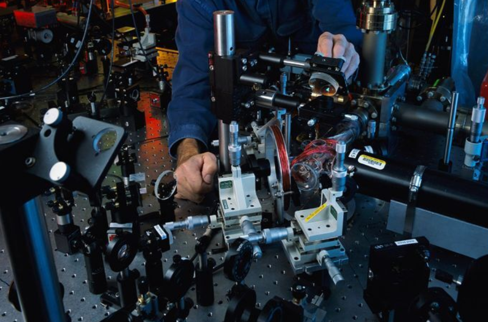
At present, CPO is still in its infancy, and there are still problems such as low yield and high maintenance costs, and few manufacturers on the market can fully provide CPO related products. Only Broadcom, Marvell, Intel, and a handful of other players have fully proprietary solutions on the market.
Marvell introduced a 2.5D CPO technology switch using the VIA-LAST process last year. After the silicon optical chip is processed, the TSV is processed with the processing capability of OSAT, and then the electrical chip flip-chip is added to the silicon optical chip. 16 optical modules and switching chip Marvell Teralynx7 are interconnected on the PCB to form a switch, which can achieve a switching rate of 12.8Tbps.
At this year’s OFC, Broadcom and Marvell also demonstrated the latest generation of 51.2Tbps switch chips using optoelectronic co-packaging technology.
From Broadcom’s latest generation of CPO technical details, CPO 3D package through the improvement of the process to achieve a higher I/O density, CPO power consumption to 5.5W/800G, energy efficiency ratio is very good performance is very good. At the same time, Broadcom is also breaking through to a single wave of 200Gbps and 102.4T CPO.
Cisco has also increased its investment in CPO technology, and made a CPO product demonstration in this year’s OFC, showing its CPO technology accumulation and application on a more integrated multiplexer/demultiplexer. Cisco said it will conduct a pilot deployment of CPO in 51.2Tb switches, followed by large-scale adoption in 102.4Tb switch cycles
Intel has long introduced CPO based switches, and in recent years Intel has continued to work with Ayar Labs to explore co-packaged higher bandwidth signal interconnection solutions, paving the way for the mass production of optoelectronic co-packaging and optical interconnect devices.
Although pluggable modules are still the first choice, the overall energy efficiency improvement that CPO can bring has attracted more and more manufacturers. According to LightCounting, CPO shipments will start to increase significantly from 800G and 1.6T ports, gradually begin to be commercially available from 2024 to 2025, and form a large-scale volume from 2026 to 2027. At the same time, CIR expects that the market revenue of photoelectric total packaging will reach $5.4 billion in 2027.
Earlier this year, TSMC announced that it will join hands with Broadcom, Nvidia and other large customers to jointly develop silicon photonics technology, common packaging optical components CPO and other new products, process technology from 45nm to 7nm, and said that the fastest second half of next year began to meet the large order, 2025 or so to reach the volume stage.
As an interdisciplinary technology field involving photonic devices, integrated circuits, packaging, modeling and simulation, CPO technology reflects the changes brought by optoelectronic fusion, and the changes brought to data transmission are undoubtedly subversive. Although the application of CPO may only be seen in large data centers for a long time, with the further expansion of large computing power and high bandwidth requirements, CPO photoelectric co-seal technology has become a new battlefield.
It can be seen that manufacturers working in CPO generally believe that 2025 will be a key node, which is also a node with a exchange rate of 102.4Tbps, and the disadvantages of pluggable modules will be further amplified. Although CPO applications may come slowly, opto-electronic co-packaging is undoubtedly the only way to achieve high speed, high bandwidth and low power networks.
Post time: Apr-02-2024