


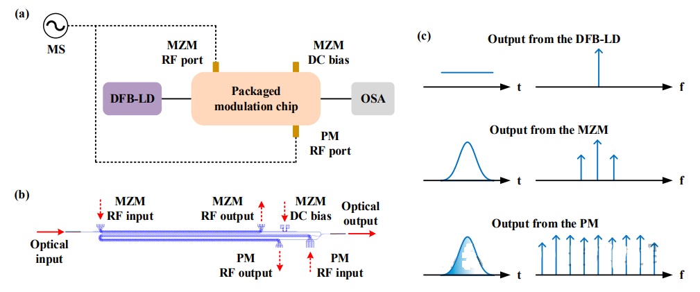
A scheme of optical frequency thinning based on MZM modulator
The optical frequency dispersion can be used as a liDAR light source to simultaneously emit and scan in different directions, and it can also be used as a multi-wavelength light source of 800G FR4, eliminating the MUX structure. Usually, the multi-wavelength light source is either low power or not well packaged, and there are many problems. The scheme introduced today has many advantages and can be referred to for reference. Its structure diagram is shown as follows: The high-power DFB laser light source is CW light in time domain and single wavelength in frequency. After passing through a modulator with a certain modulation frequency fRF, sideband will be generated, and the sideband interval is the modulated frequency fRF. The modulator uses a LNOI modulator with a length of 8.2mm, as shown in Figure b. After a long section of high-power phase modulator, the modulation frequency is also fRF, and its phase needs to make the crest or trough of the RF signal and the light pulse relative to each other, resulting in a large chirp, resulting in more optical teeth. The DC bias and modulation depth of the modulator can affect the flatness of the optical frequency dispersion.
Mathematically, the signal after the light field is modulated by the modulator is:
It can be seen that the output optical field is an optical frequency dispersion with a frequency interval of wrf, and the intensity of the optical frequency dispersion tooth is related to the DFB optical power. By simulating the light intensity passing through MZM modulator and PM phase modulator, and then FFT, the optical frequency dispersion spectrum is obtained. The following figure shows the direct relationship between optical frequency flatness and modulator DC bias and modulation depth based on this simulation.
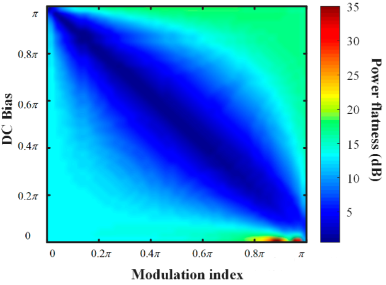
The following figure shows the simulated spectral diagram with MZM bias DC of 0.6π and modulation depth of 0.4π, which shows that its flatness is <5dB.
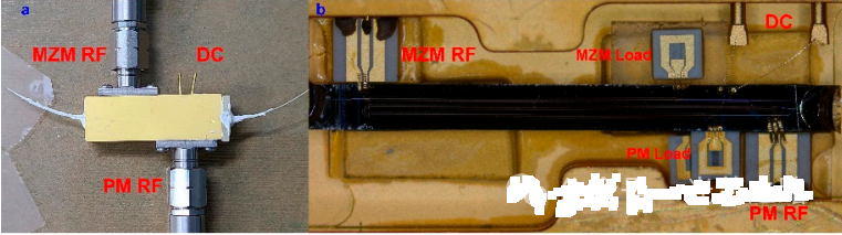
The following is the package diagram of the MZM modulator, LN is 500nm thick, the etching depth is 260nm, and the waveguide width is 1.5um. The thickness of the gold electrode is 1.2um. The thickness of the upper cladding SIO2 is 2um.
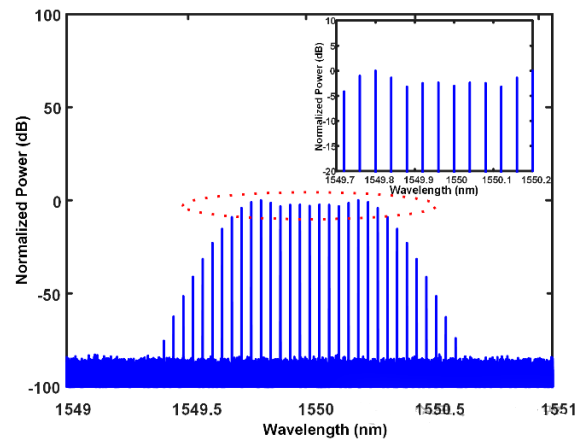
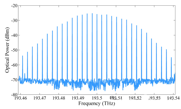
The following is the spectrum of the tested OFC, with 13 optically sparse teeth and flatness <2.4dB. The modulation frequency is 5GHz, and the RF power loading in MZM and PM is 11.24 dBm and 24.96dBm respectively. The number of teeth of optical frequency dispersion excitation can be increased by further increasing the PM-RF power, and the optical frequency dispersion interval can be increased by increasing the modulation frequency. picture
The above is based on LNOI scheme, and the following is based on IIIV scheme. The structure diagram is as follows: The chip integrates DBR laser, MZM modulator, PM phase modulator, SOA and SSC. A single chip can achieve high performance optical frequency thinning.
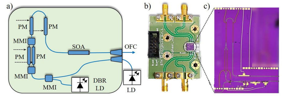
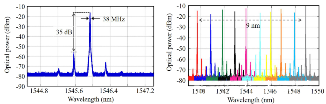
The SMSR of the DBR laser is 35dB, the line width is 38MHz, and the tuning range is 9nm.
The MZM modulator is used to generate sideband with a length of 1mm and a bandwidth of only 7GHz@3dB. Mainly limited by impedance mismatch, optical loss up to 20dB@-8B bias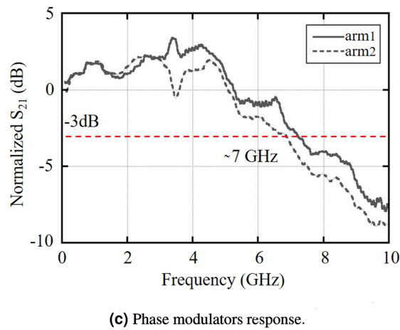
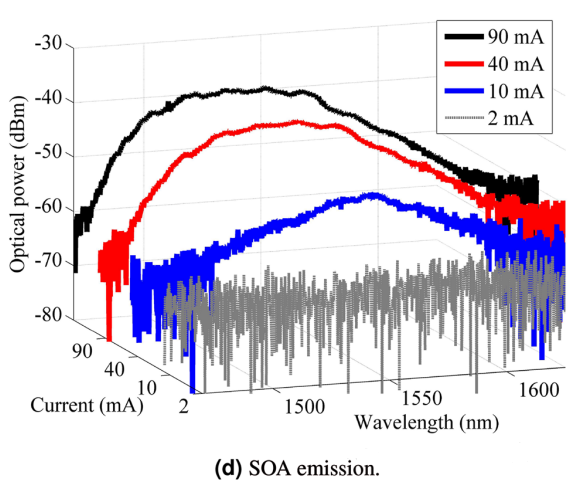
The SOA length is 500µm, which is used to compensate the modulation optical difference loss, and the spectral bandwidth is 62nm@3dB@90mA. The integrated SSC at the output improves the coupling efficiency of the chip (coupling efficiency is 5dB). The final output power is about −7dBm.
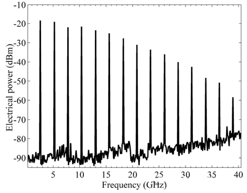
In order to produce optical frequency dispersion, the RF modulation frequency used is 2.6GHz, the power is 24.7dBm, and the Vpi of the phase modulator is 5V. The figure below is the resulting photophobic spectrum with 17 photophobic teeth @10dB and SNSR higher than 30dB.
The scheme is intended for 5G microwave transmission, and the following figure is the spectrum component detected by the light detector, which can generate 26G signals by 10 times the frequency. It is not stated here.
In summary, the optical frequency generated by this method has stable frequency interval, low phase noise, high power and easy integration, but there are also several problems. The RF signal loaded on the PM requires large power, relatively large power consumption, and the frequency interval is limited by the modulation rate, up to 50GHz, which requires a larger wavelength interval (generally >10nm) in the FR8 system. Limited use, power flatness is still not enough.
Post time: Mar-19-2024